-
Products
-
Filters
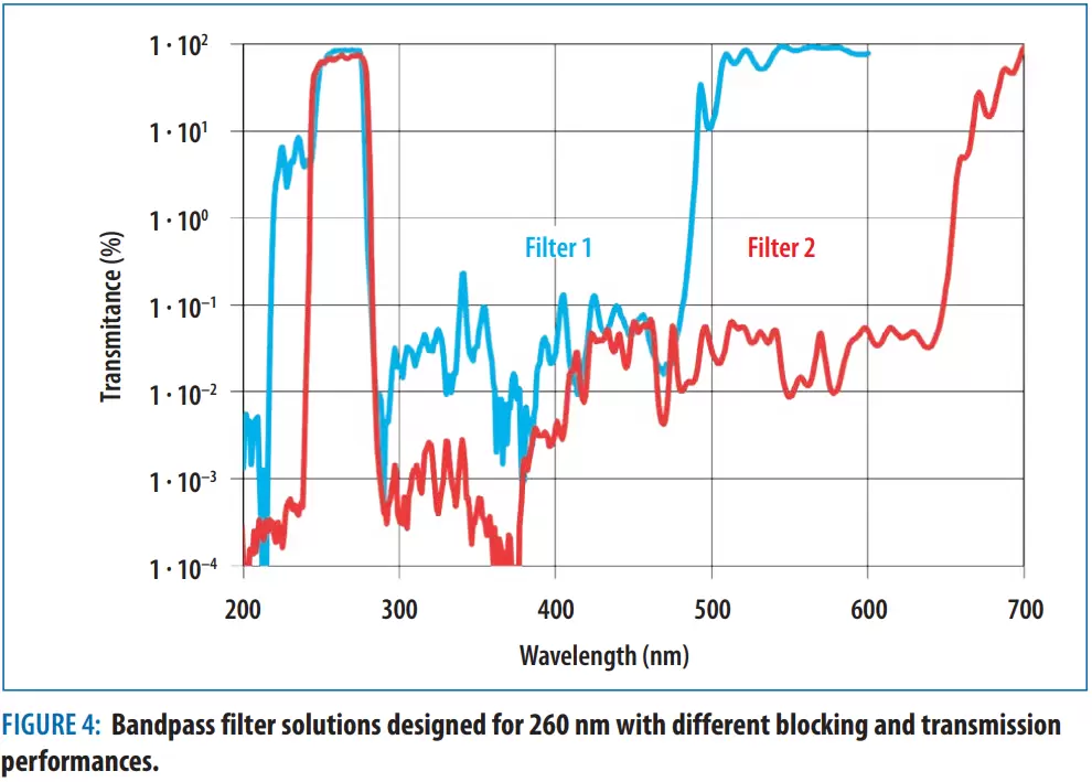
- Bandpass Filters
- Narrow Bandpass Filters
- NIR Bandpass Filters
- SWIR Bandpass Filters
- Calflex™ Heat Protection Filters
- Calflex™ 3000 SP
- Conversion Filters
- Dichroic Filters
- Patterned Dichroic Filters
- Dichrolight™
- Dichrolight™ Patterned Filters
- Fluorescence Filter Sets
- GoboXtreme™ Animation Wheel
- GoboXtreme™ Dark
- IR-Blocking Filters
- Laser Safety Filters
- LED ColorDichroics™
- Linear Variable Filters
- NightVision™ Filters
- Notch Filters
- Raman Filters
- SoFi™ Solar Filters
- UV-Filters
- UV-Guard™
- UV/IR-Blockers
- Mirrors
- Prisms
- Micro Optics
- Lids / Windows
- Splitters / Combiners
- Patterned Products
- Customized Products
-
Filters
- Coatings
- CoatingPlus™
-
Applications
- Adaptive Cruise Control
- Aerospace Cockpit
- Ambient Light Sensing
- Autonomous vehicles
- Barcode Reading
- Beam steering
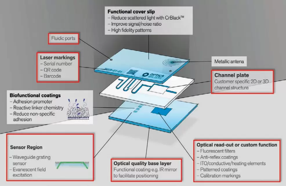
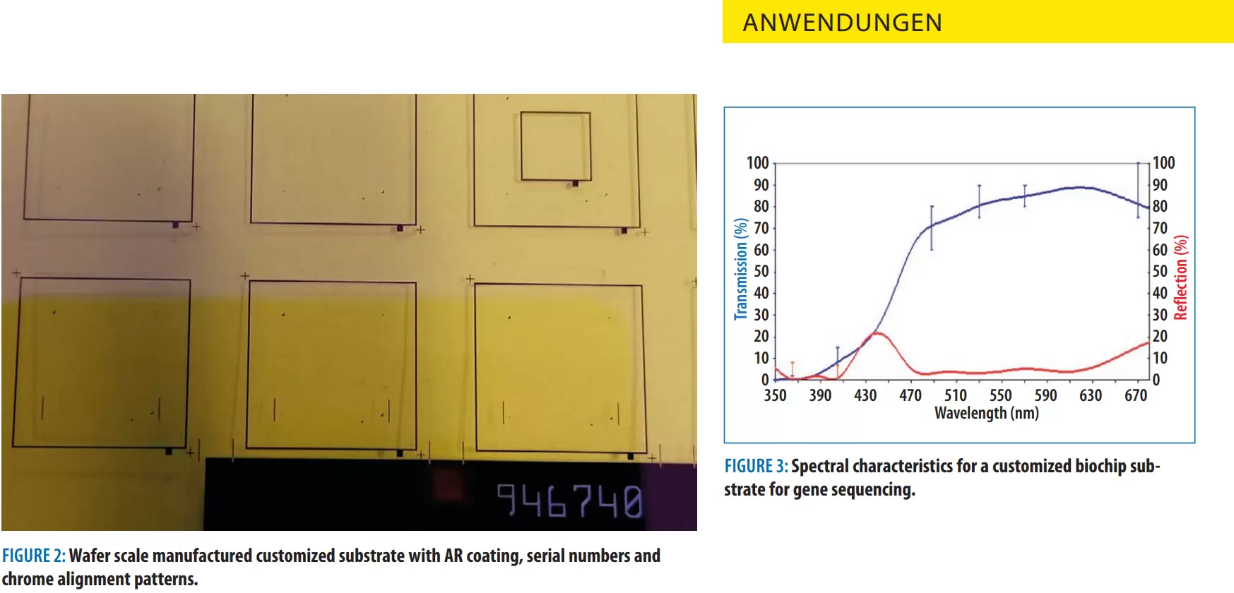
- Biochip Applications
- Camera – Optical Imaging
- Color Temperature Measurement
- Currency recognition
- Data Collection
- Driver Assistance Camera
- Earth Observation
- Endoscopic applications
- Entertainment Lighting
- Facial Recognition
- Flow Cells
- Food Industry & Agriculture
- Fluorescence Detection
- Gas Sensing
- Gesture Recognition and Control
- HD & Tele Camera
- Head-Up Displays
- Health Monitoring
- Hyperspectral imaging
- Image Sensors – Cover Lids
- Image Sensors - Multispectral
- Inspection cameras
- Intelligent Headlights
- Intra-Oral Scanner
- Laser Beam Scanning (LBS) Displays
- Laser Beam Sources
- Laser Blocking Filters
- LED Systems
- Light Curtains
- Light management
- Manufacturing
- Material Processing
- Medical Lighting
- Micromachining
- Microscopy
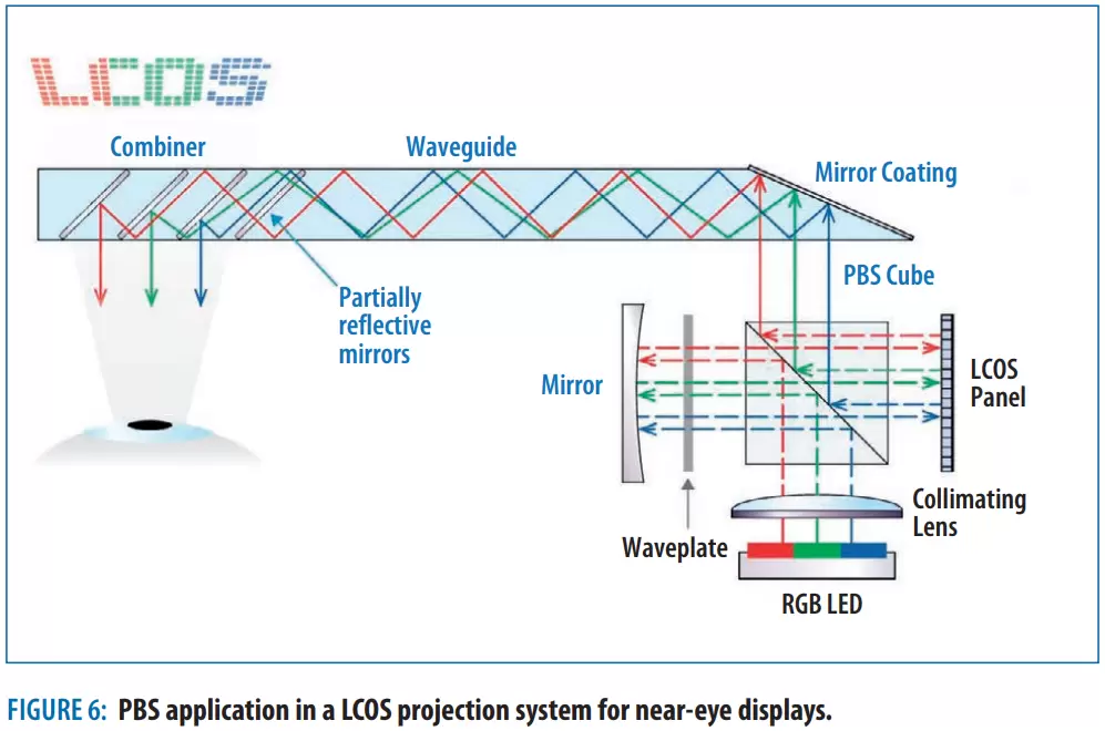
- Near-Eye Displays
- Night Vision Systems
- Ophthalmologic Surgery
- Positioning systems
- Printing & Painting Industry
- Projection Display – Portable & Embedded
- Projection Display – Large Venue & Cinema
- Raman Spectroscopy
- Range Finder
- Remote Multi-Spectral Imaging
- Ring Laser Gyroscope
- Robotics
- Scanning LiDAR and Solid State LiDAR
- Spectroscopy
- Storehouse management
- Sun simulation
- Super Resolution Microscopy
- Surveillance cameras
- Technical Lighting
- Traffic control
- UV Curing
- UV Illumination
- Wafer Inspection
- Waste Sorting
- Water analysis
- 3D Mapping / Gesture Recognition
- Markets