arrow

Manufacturing interdigital electrodes for capacitive sensing

1/3

Materion Balzers Optics Logo
Manufacturing interdigital electrodes for capacitive sensing

Application Note
MBO-AE-002 (2401-1)

Optics Balzers AG

Neugrüt 35
LI-9496 Balzers
T +423 388 9200
www.materionbalzersoptics.com

Materion Balzers Optics has been the innovative and independent industry partner for the development and production of coated optical components and subassemblies for more than 70 years.

Manufacturing interdigital electrodes for capacitive
sensing using thin film deposition


Authors: Reto Keller, Business Development Manager at Optics Balzers AG, Balzers, Liechtenstein


Materion Balzers Optics apabilities in metallic thin film deposition and lithographic patterning enable the fabrication of interdigital electrodes and meandering wires on glass for a wide variety of applications. These planar electrodes and resistors are among the most widely used periodic structures in many sensor and transducer designs. This is thanks to their versatility and to their ability to utilize multiple physical effects with the same type of geometric structure. With our expertise and leading process technology we enable our customers to develop advanced sensors, thereby integrating additional functions into their optical systems.

Interdigital capacitive sensors (IDC-S) and transducers (IDC-T)
When a voltage is applied to an interdigital electrode, it forms a capacitance with a fringing electric field across the metallic structures. The impedance of this interdigital electrode circuit can be measured, thus providing a sensor device capable of gauging changes in the dielectric properties of materials penetrated by the electric field lines. This type of dielectrometrical sensors is used to monitor the curing process of polymer-based resins or in nondestructive material testing. In general, the sensors are suitable for all applications in which changes in the material under test (MUT) can be measured as changes in the dielectric properties of said material. However, many of these sensors still use parallel plate capacitance probes (Fig. 2a) which can be cumbersome. Due to their planar nature, using interdigital electrodes instead of parallel probes can simplify the design and handling of dielectrometrical sensors.

Interdigital electrodes are also suitable for the design of magnetic field and piezo-acoustic sensors. Magnetic field sensors can be used in applications such as the detection of early fatigue and cracks in components made of aluminum and stainless steel. Piezo-acoustic IDC sensors and transducers can be found in Surface Acoustic Wave (SAW) devices, which work as high frequency filters such as those used in mobile phone receivers.

Finally, for transducer applications, the fringing electric field induced through the interdigital electrodes is also able to generate mechanical forces. This capability makes them a feasible choice for the actuation of moving parts in the order of tens of micrometers, for example in a microelectromechanical system (MEMS) device.

Fig. 1a. Elements of an Interdigital Electrode, Fig. 1b. Example of a Meander-Line Resistor, Fig. 2a. Fringing field dielectrometric sensors with parallel plate electrodes, Fig. 2b. Fringing field dielectrometric sensors with planar interdigital electrodes


Copyright: The information provided herein is correct to the best of Materion Balzers Optics knowledge. No liability for any errors, facts or opinions is accepted. Materion Balzers Optics disclaims any liability for incidental or consequential damages, which may result from the use of the product that are beyond its control. Nothing contained herein is to be considered as permission or a recommendation to infringe any patent or any other intellectual property right. All information contained herein is subject to change without notice. www.materionbalzersoptics.com


2/3

Materion Balzers Optics Logo

Easy application and greater flexibility
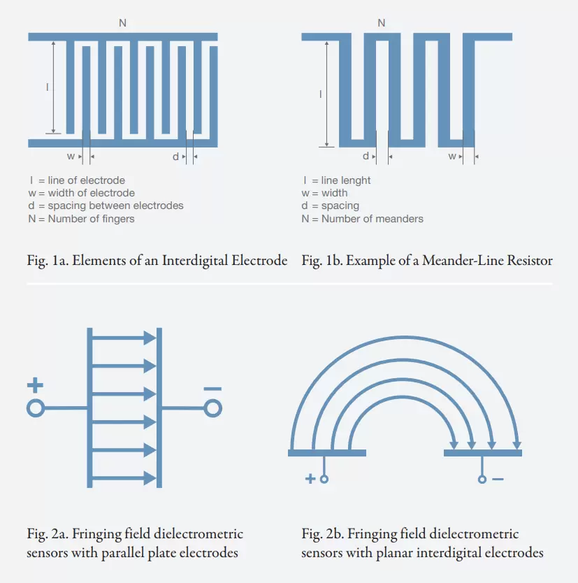
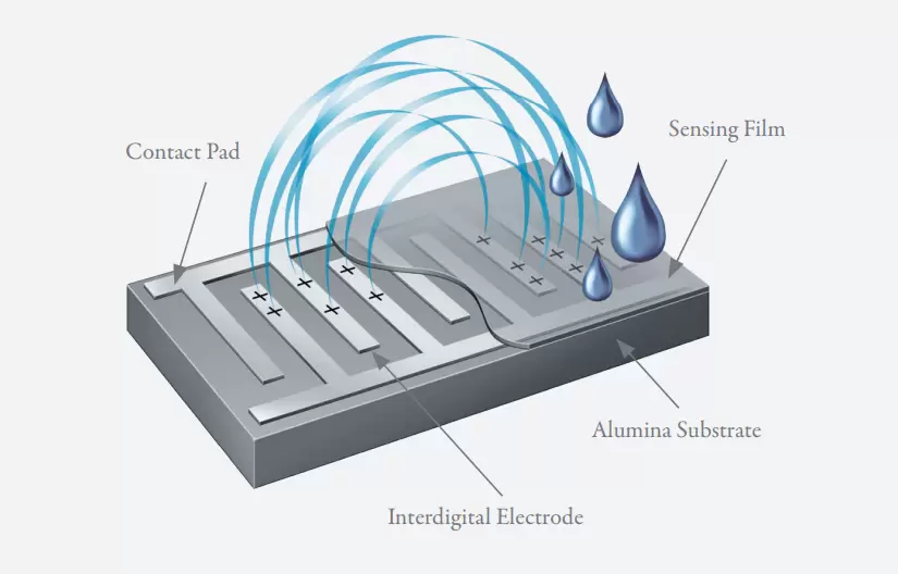
An inherent advantage of the planar arrangement of the interdigital electrodes over a parallel plate configuration is that only single-sided access to a MUT is required (Fig. 2b). This eliminates the need to place the electrodes on opposing sides of the MUT. It also makes IDC sensors suitable for a number of applications where they can simply be applied laterally to a test specimen.

Interdigital electrodes allow for extremely flexible design of sensor devices. To meet specific application requirements, the sensitivity of such a device can be altered by changing any of the following (Figures 1a and 1b):

– the overall effective electrode area
– the number of metallic fingers
– the spacing between the electrodes
– the dielectric material between the electrodes.

These possibilities allow customers to easily optimize sensor layouts for their specific applications.

4 steps to produce interdigital electrode or meander wire resistor structures
Thin film deposition and lithography processes are our core competencies. We have optimized these processes for the fabrication of both capacitive and resistive sensor elements, such as interdigital electrodes or meandering resistors on thin glass or quartz substrates, supporting feature sizes as low as 5µm. The production process can be broken down into four major steps.

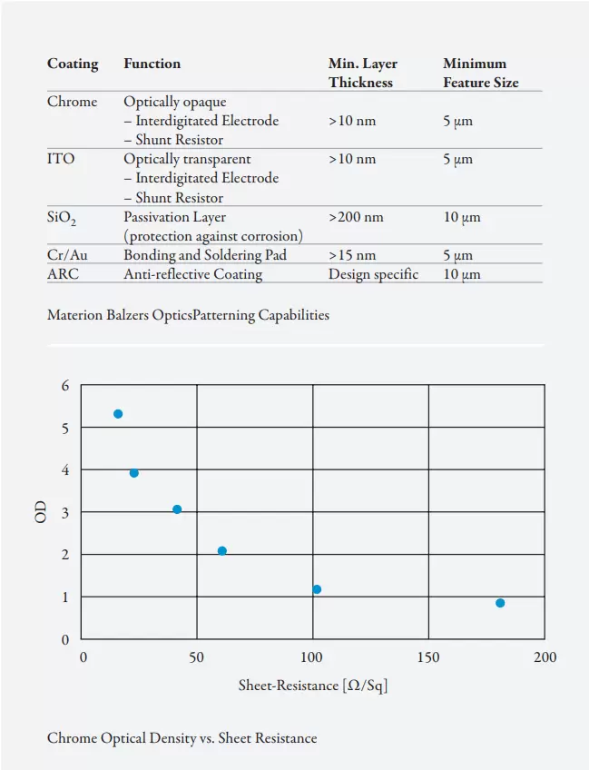
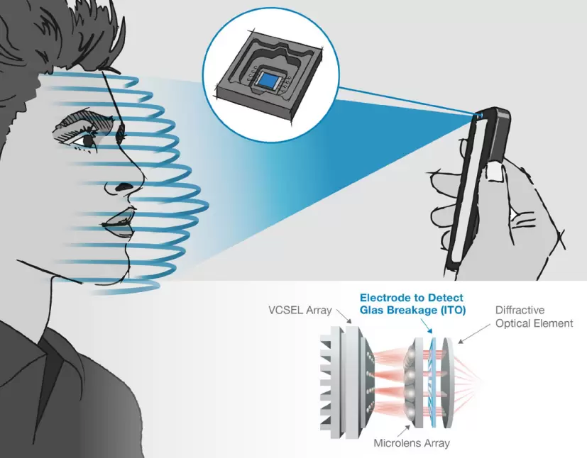
First, the conductive electrode material is applied to the target substrate by magnetron sputtering. Materion Balzers Optics is a world leader in this technology, which allows us to produce sensors and transducers cost-effectively and in very large quantities. For opaque electrodes, chrome is usually used as the electrode material. If a sensor needs to be placed into the optically active area, indium tin oxide (ITO) allows us to produce transparent structures instead. With our sophisticated process control, the layer resistance of our chrome coating can be controlled within a tolerance window of ±2.5%, resulting in consistent sensor quality even in high volume production.

Once the conductive electrode material has been applied, lithography is used to structure this first layer. Depending on the design, we apply an etching or a lift-off process that allows features to be made as thin as 5μm. In order to protect them against corrosion, the metallic electrodes are subsequently covered with a passivation layer of SiO₂. In a second patterning step this layer is opened again in order to add contact area for solder or bond pads to connect to the electrode structures.

Finally, in a third coating run and litho step, the gold and chromium materials are deposited and structured to form the solder or bond pads. These pads then connect the sensor electrodes with a suitable signal amplifier to an external circuit.

Prepared for high volume production
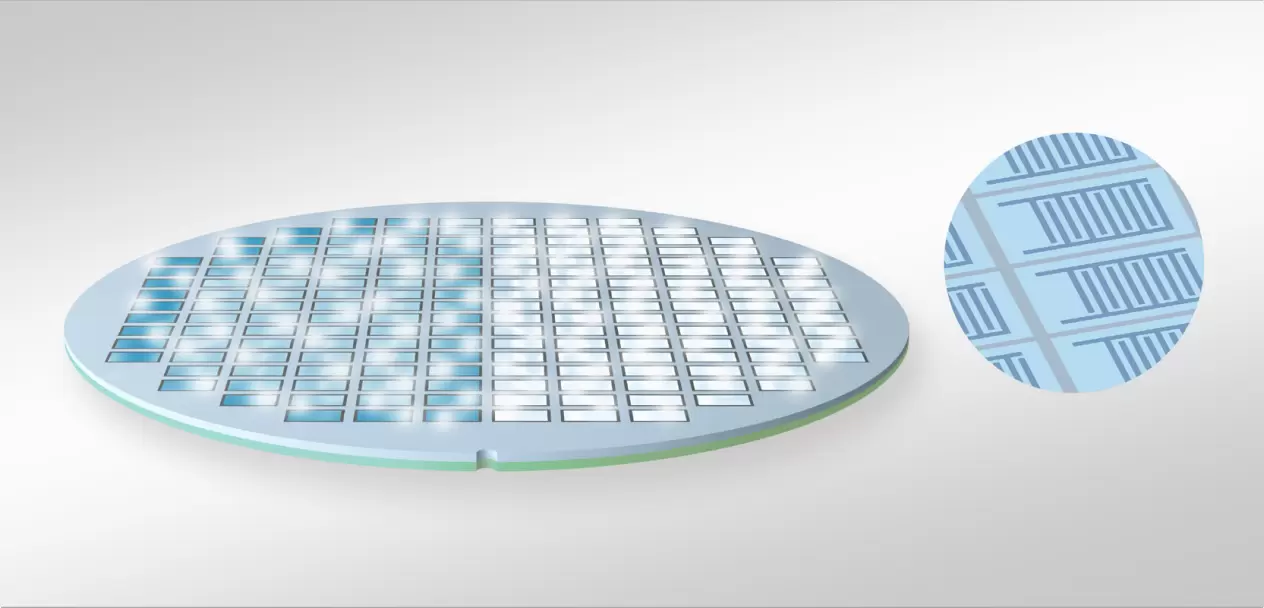
As a market leader, Materion Balzers Optics can produce in volume, consistently ensuring low tolerances and thus superior quality. All manufacturing processes are scalable for mass production, with parallel processing of thousands of sensor elements on a single glass wafer. Fully automated dicing enables Materion Balzers Optics to deliver large quantities of sensor elements in wafer packages or on wafer rings. After dicing, each individual sensor undergoes automated optical inspection. In addition, continuous optimization of the production process after the first ramp-up maximizes the yield and further reduces cost.

Materion Balzers OpticsPatterning Capabilities & Chrome Optical Density vs. Sheet Resistance

Practical applications
There is a broad spectrum of existing and new applications for planar interdigital electrodes on glass from Materion Balzers Optics.

A common application for interdigital electrodes is to measure the concentration of chemicals in a gas or liquid. Using a suitable sensing film that reacts to the specific chemical substance, a change in the dielectric properties indicates a rising or falling concentration of the specific chemical. For example, using a sensor film that interacts with water creates a humidity sensor which can be integrated into weather stations, industrial devices, IoT systems or mobile phones (Fig. 3). Such humidity sensors can be built with different film materials such as SiO₂ or a number of polymeric films.

In view of climate change, equally important are sensors to measure CO₂ concentration in the air. Sensing films made of inorganic semiconductor oxides or organic polymers can be used for this, particuler application to measure the concentration of chemical gases.

Other common applications for interdigital electrodes include non-destructive testing, biotechnology or microelectromechanical systems (MEMS).


Copyright: The information provided herein is correct to the best of Materion Balzers Optics knowledge. No liability for any errors, facts or opinions is accepted. Materion Balzers Optics disclaims any liability for incidental or consequential damages, which may result from the use of the product that are beyond its control. Nothing contained herein is to be considered as permission or a recommendation to infringe any patent or any other intellectual property right. All information contained herein is subject to change without notice. www.materionbalzersoptics.com


3/3

Materion Balzers Optics Logo

New applications with ITO-based electrodes
Interdigital electrodes from Materion Balzers Optics also enable completely new applications such as the automatic detection of glass breakage. This can be very important for the 3D face recognition technology used in today’s smartphones, where a VCSEL laser is used in conjunction with a diffraction element which generates the required infrared light pattern. A break in this diffraction element could expose the human eye to the un-diffracted laser beam, potentially causing serious injury. In such a case, a sensor for broken glass based on interdigital electrodes would experience a change of dielectric permittivity due to cracks in the diffraction element (Fig. 4) and could be used to switch off the laser immediately. In this application, the interdigital electrodes need to be brought into the optical path and must therefore be optically transparent. Materion Balzers Optics has a deep understanding of transparent electrodes and has developed advanced production processes for such devices.

Conclusion
Interdigital electrodes have been adopted in an immense variety of sensor applications due to their versatility, their relatively straightforward design which allows one-sided access to the MUT, and the mature production processes, enabling high volume production at low cost. As a global leader in the supply of optical coatings and components, Materion Balzers Optics has developed and optimized these processes over decades, providing its customers with outstanding quality and above average yields.

With layers as thin as 10nm and feature sizes as low as 5µm, Materion Balzers Optics can fulfill almost any capacitive or resistive pattern design. Where there are very specific requirements, our highly experienced and skilled development and engineering teams collaborate closely with customers to develop and deliver innovative solutions. Whether it is non-destructive testing, moisture and gas sensing, process control or any other application, Materion Balzers Optics has the technology and the processes in place to manufacture precisely to customer specifications.

Fig. 3 . Change of dielectric permitivity ε due to humidity change

Fig. 3 . Change of dielectric permitivity ε due to humidity change


Fig. 4. VCSEL for facial recognition for mobile devices

Fig. 4. VCSEL for facial recognition for mobile devices


Copyright: The information provided herein is correct to the best of Materion Balzers Optics knowledge. No liability for any errors, facts or opinions is accepted. Materion Balzers Optics disclaims any liability for incidental or consequential damages, which may result from the use of the product that are beyond its control. Nothing contained herein is to be considered as permission or a recommendation to infringe any patent or any other intellectual property right. All information contained herein is subject to change without notice. www.materionbalzersoptics.com